Enabling next-gen electronics with precision and reliability
Project Overview
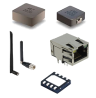
To develop comprehensive technical assets—including Product datasheets, 3D models, and Technical Sales drawings—for Frequency Control& Timing Devices, RF & Antennas, Power & Magnetic electronic components. These deliverables support product integration, customer designworkflows, and PCB symbols and footprints readiness across industries such as automotive, and industrial automation.
Design Requirements
- Accurate Dimensions: Include full body dimensions, lead/pin geometry, and tolerances.
- Mounting Features: Show pad layout, soldering zones, and keep-out areas, through-holes, or mechanical clips asper antenna type(chip, PCB trace, SMA connector).
- Form Factor Constraints: Work within fixed PCB layouts, enclosures, and mechanical boundaries.
- Connector Standards: Match SMA, MMCX, U.FL, or custom RF connectors already in use.
- Exact Dimensions: Model antennas using datasheet specs (length, width, height, pin pitch, pad size).
- Ensuring symbolic consistency with IEEE-315:1993 standards for schematic clarity and cross-disciplinary communication.
Key Tools
Operating System:Windows
Tools:
- MS Office
- SolidWorks
- AutoCAD
Project Deliverables
- 3D Model Formats: Providing STEP, Model & Drawing files, and native CADformats, PDFs and 3D PDFs.
- SCD document files..
- Frequency Data Plot Graph files.
- PCB and Schematic files.
- ECN/EOL Documents.
Outcome / Results
- Delivered manufacturing solutions that support the development of next-generation electroniccomponents with ultra-high precision and consistent performance.
- Ensured micron-level accuracy and flawless repeatability, resulting in higher reliability, longerproduct life, and reduced failure rates in advanced electronics
- Provided robust, scalable manufacturing systems capable of meeting high-volume demand whilemaintaining strict quality standards.
Learning & Future Scope
- Understanding precision fabrication techniques for semiconductors, PCBs, MEMS, andmicroelectronics.
- Learning techniques to manage thermal, electrical, and mechanical tolerances at micro- and nano-scales.
- Exposure to global standards and best practices in electronics manufacturing.
- Increased demand for ultra-precise, high-reliability manufacturing solutions.
- Development of eco-friendly processes, energy-efficient equipment, and reduced material waste.